


MTW European Type Trapezium Mill
Input size:30-50mm
Capacity: 3-50t/h
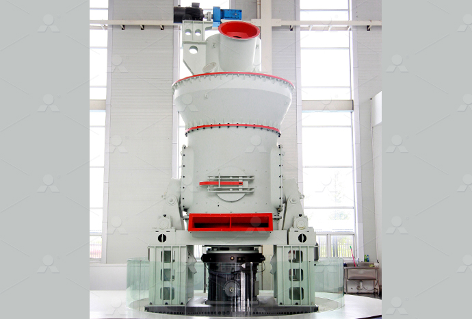
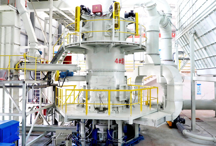
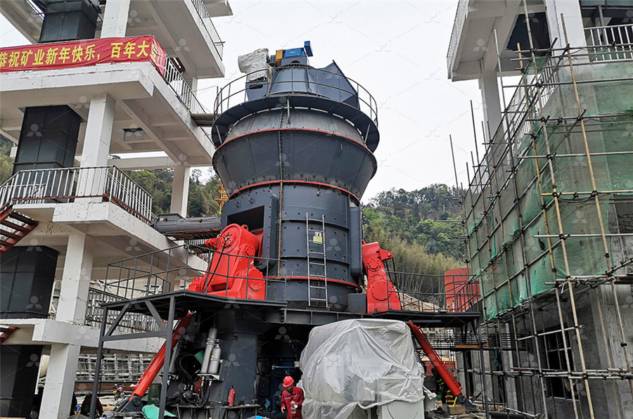
LM Vertical Roller Mill
Input size:38-65mm
Capacity: 13-70t/h
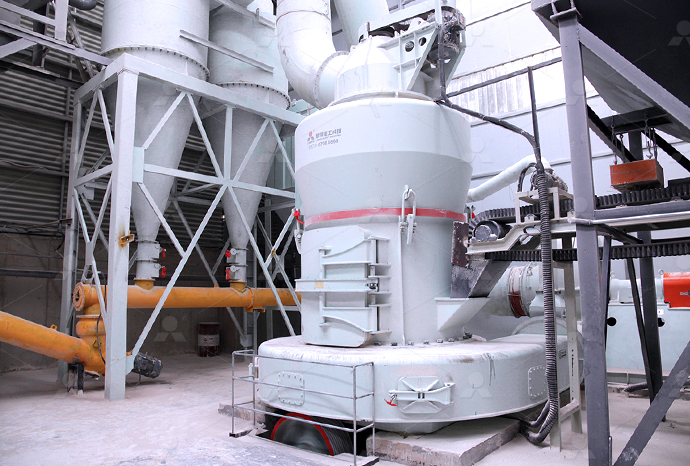
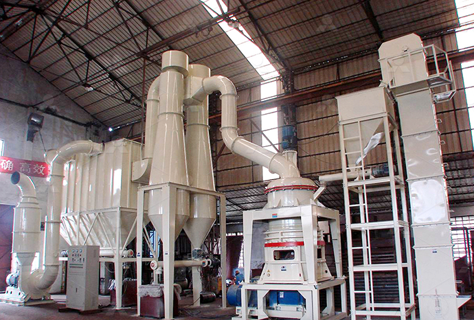
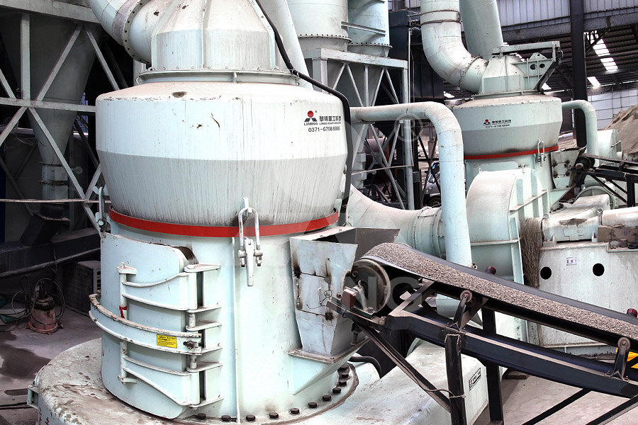
Raymond Mill
Input size:20-30mm
Capacity: 0.8-9.5t/h
Sand powder vertical mill
Input size:30-55mm
Capacity: 30-900t/h
LUM series superfine vertical roller grinding mill
Input size:10-20mm
Capacity: 5-18t/h
MW Micro Powder Mill
Input size:≤20mm
Capacity: 0.5-12t/h

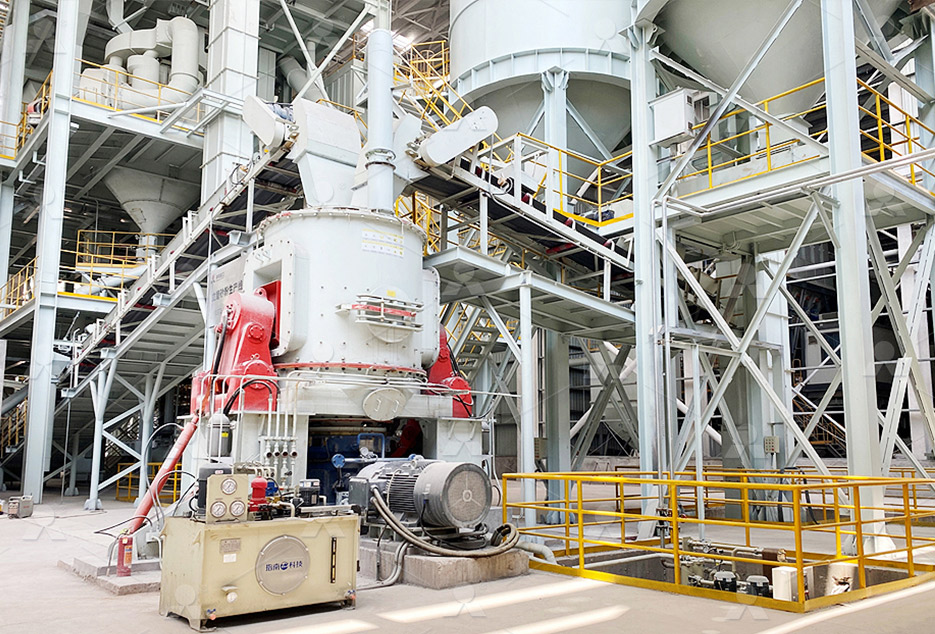
LM Vertical Slag Mill
Input size:38-65mm
Capacity: 7-100t/h
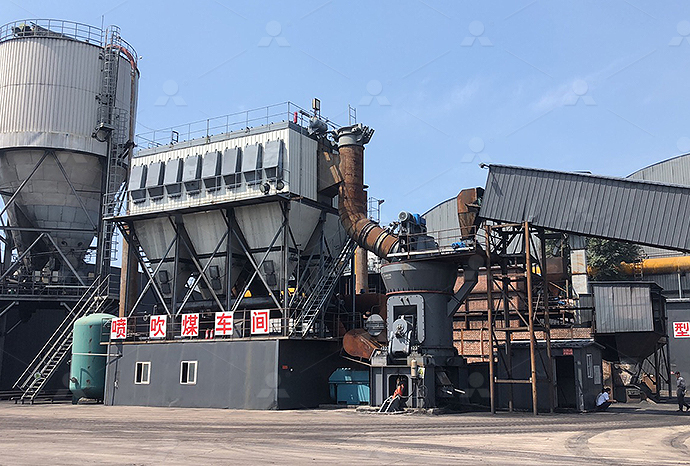
LM Vertical Coal Mill
Input size:≤50mm
Capacity: 5-100t/h
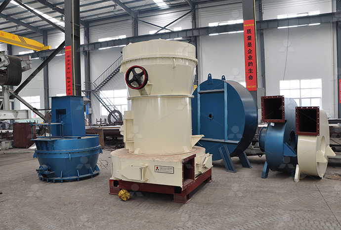
TGM Trapezium Mill
Input size:25-40mm
Capacity: 3-36t/h
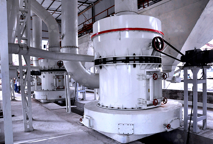
MB5X Pendulum Roller Grinding Mill
Input size:25-55mm
Capacity: 4-100t/h
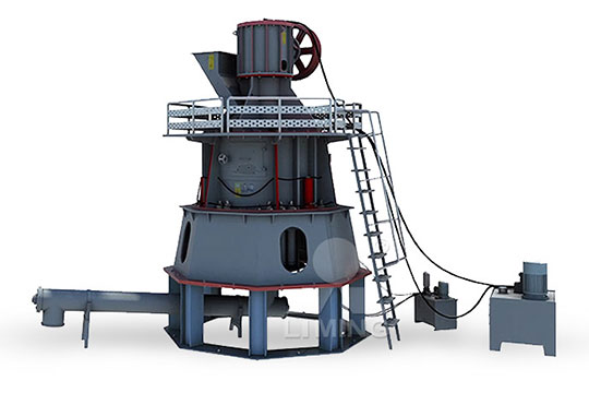
Straight-Through Centrifugal Mill
Input size:30-40mm
Capacity: 15-45t/h
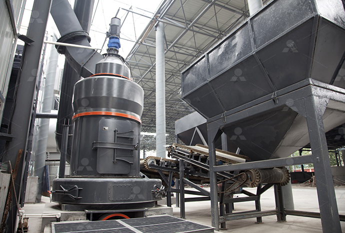
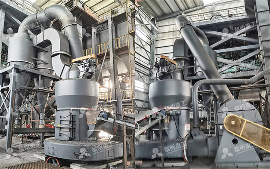
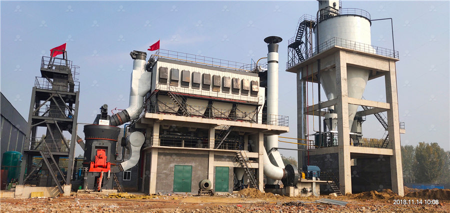
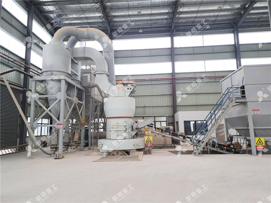
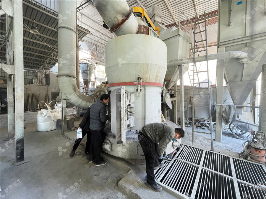
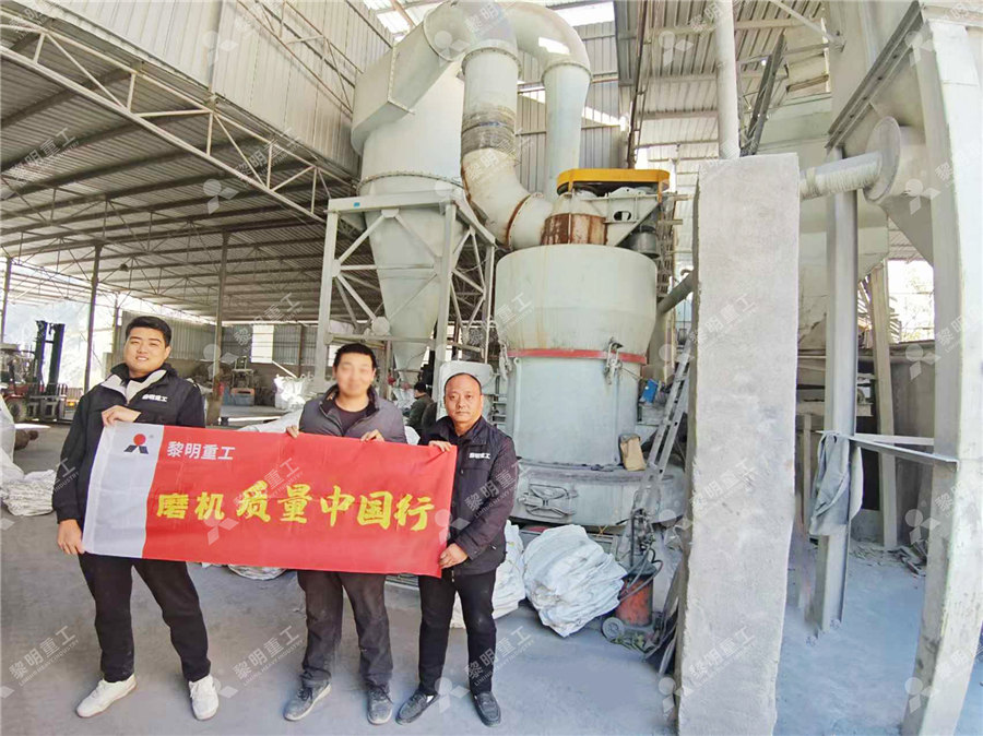
Processing silicon dioxide machine
Experimental Set Up to Improve Machining Performance of Silicon
2018年4月21日 This study focuses on the development of magnetic field assisted traveling wire electrochemical spark machining (MFTWECSM) process set up and its utilization for the 2019年8月23日 Also called silica sand or quartz sand, silica is made of silicon dioxide (SiO 2) Silicon compounds are the most significant component of the Earth’s crust Since sand is plentiful, easy to mine and relatively easy to Silica Processing Equipment, Process Flow, Cases2024年9月7日 Silicon wafers are made through a process called Czochralski growth, where a silicon crystal is pulled from molten silicon and then sliced into thin wafers What are the key steps in silicon wafer fabrication?Silicon Wafer Manufacturing Process: Sand to Silicon2017年6月5日 The oxidation process creates an SiO2 layer, which serves as an insulating layer that blocks leakage current between circuits The oxide layer also protects the silicon wafer during the subsequent ion implantation and etching The oxidation process Samsung Semiconductor Global
Electrical discharge machining process investigation
2024年4月6日 This research paper explores the impact of electrical discharge machining process parameters, including current, pulseon time (Ton), and pulseoff time (Toff), on the material removal rate (MRR) and surface roughness Refractive index is a good indicator of film composition, ie Si:N ratio or Si:O ratio It can be easily measured by ellipsometer or prism coupler, allowing rapid evaluation of film composition (and Basic PECVD Plasma Processes (SiH based) University of 2017年4月12日 Silicon Travelling wire electrochemical spark machining (TWECSM) has the potential for the machining of advanced nonconducting materials like glass, quartz, silicon Experimental Investigations and Multiresponse Optimization of The whole of planar electronics processing and the modern IC industry has been made possible by the unique properties of silicon dioxide It is the only native oxide of a common semiconductor which is stable in water and at elevated temperatures, an excellent electrical insulator, a mask to common diffusing species, and capable of forming a nearly perfect electrical interface with its SiO2: Properties and Applications Enigmatics
Silicon Planar Processing and Photolithography SpringerLink
2016年7月31日 From a nanofabrication standpoint, once a single crystal cylindrical ingot of silicon is grown and cut into circular wafers (roughly 12 inches in diameter and 05 mm thick at present and most often covered with a submicron layer of silicon dioxide or other dielectrics), the principal patterning step (2) that generates nanoscale features in the lateral dimension is Silicone processing equipment and techniques Silicone is a synthetic material composed of silicon, oxygen, carbon, and hydrogen Being one of the main ingredients in silicone, the chemical element silicon is most commonly found Silicone making equipment Making2015年1月1日 Oxygen is in interstitial sites in silicon lattice, and in CZ silicon it is supersaturated at normal processing temperatures The typical achievable range in CZ growth process is approximately 6–18 ppma, or 3–9×10 17 atoms/cm 3 Si expressed in Silicon Wafers: Preparation and Properties ScienceDirectStrain Measurements of Silicon Dioxide Microspecimens by Digital Imaging Processing WN Sharpe Jr J Pulskamp DS Gianola C Eberl RG Polcawich RJ Thompson Received: 25 July 2006 /Accepted: 21 September 2006 / Published online: 3 February 2007 # Society for Experimental Mechanics 2007 Abstract Silicon dioxide thin film is a Strain Measurements of Silicon Dioxide Microspecimens by
(PDF) Advanced Plasma Processing: Etching, Deposition, and
2010年4月1日 Plasma processing techniques are one of the cornerstones of modern semiconductor fabrication al, 2009) Silicon dioxide masks typically off er high selectivity (150:1 for Bosch and 200:1 for 2023年11月20日 You are accessing a machinereadable page In order to be humanreadable, Synthesis and Application of Silicon Dioxide Nanoparticles The Article Processing Charge (APC) for publication in this open access journal is 2900 CHF (Swiss Francs)Synthesis and Application of Silicon Dioxide Nanoparticles2024年3月1日 Owing to its high carrier mobility, large bandgap, and good thermal conductivity, singlecrystal silicon carbide (SiC) is commonly used to fabricate highpower devices [1, 2]However, the hardness of SiC is second only to that of diamond, and its high brittleness and strong chemical inertness pose significant challenges to the ultraprecision machining of its Compound mechanical and chemicalmechanical polishing processing Summary Many processing steps are required to fabricate complex electronic devices, including doping by ion implantation, patterning, etching, Device Processing of Silicon Carbide Tsunenobu Kimoto, Tsunenobu Kimoto Kyoto University, Japan for more papers by this author James A Cooper, James A CooperDevice Processing of Silicon Carbide Wiley Online Library
R)8OC`6F[ZIB.jpg)
3M Lapping and Polishing Films for Precision Processing and
cleaner process than slurry, ability to run in CNC machine 578XA Cerium Oxide (size confidential) Polishing of cover glass edges and glass components Glass and silicon wafers 9” x 12” sheets with PSA Higher cut rates, controlled removal, conformable to edge shape, cleaner process than slurry, ability to run in CNC machine 677XA Diamond 345um2023年8月10日 A cationic collector is added to the silica sand slurry, making mica and feldspar minerals hydrophobic and forming a froth layer The froth layer is skimmed off the surface of the flotation cell The remaining particles are Silica Processing Plant 4 Major Stages to Make Silica 2007年2月3日 Silicon dioxide (SiO 2) is an integral part of the integrated circuit and microelectromechanical systems (MEMS) architectureThe ability to thermally grow high quality oxide films coupled with the insulating properties of SiO 2 has spurred the technological advances of the semiconductor industry based on Si processing [1–3]Important uses for SiO 2 include Strain Measurements of Silicon Dioxide Microspecimens by Thickness measurementswere taken before and after processing; silicon and silicon dioxide etch rates as low as 2 Å/min were obtained Figure 2 Optical microscope photos of (a) SUPERCRITICAL CARBON DIOXIDE: THE NEXT GENERATION
Zircon Processing Equipment, Process Flow, Cases JXSC Machine
2019年8月26日 aJXSC mine machinery Company in China has more than 30 years professional experience at zircon sand processing, design full set zircon sand separation plant flowchart, provides complete set zircon sand mining equipment, can send an engineer to mine site for zircon sand processing machines installation and commissioning guidance256 JOURNAL OF MICROELECTROMECHANICAL SYSTEMS, VOL 5, NO 4, DECEMBER 1996 Etch Rates for Micromachining Processing Kirt R Williams, Student Member, IEEE, and Richard S Muller, Life Fellow, IEEE Abstruct The etch rates for 317 combinations of 16 ma terials (singlecrystal silicon, doped, and undoped polysilicon, several types of silicon dioxide, Etch Rates for Micromachining Processing University of 2024年2月27日 The present work deals with analyzing the effect of silicon dioxide on mechanical and thermal stability of hybrid polymer composite Compression molding is adopted to develop the hybrid composite with constant 05 wt% of graphene and varying wt% of silicon dioxide (2, 4 6 wt%) Modified hummers method is used to synthesis graphene by chemical Effect of graphene/silicon dioxide fillers addition on mechanical 2023年6月1日 Silicon is the most widely used semiconductor material in the field of integrated circuits (ICs) and photovoltaic industry due to its abundance, low cost, and remarkable synergy with silicon dioxide [1], [2], [3], [4]In the manufacture of ICs, chemical mechanical polishing (CMP) is employed as the only global planarization technology for processing silicon wafers [5, 6]High efficiency chemical mechanical polishing for silicon wafers
.jpg)
From Sand to Silicon Intel
Silicon in the form of Silicon dioxide (SiO 2) and is the base ingredient for semiconductor manufacturing Melted Silicon – scale: wafer level (~300mm / 12 inch) Silicon is purified in multiple steps to finally reach semiconductor manufacturing quality which is called Electronic Grade Silicon Electronic Grade Silicon may only2020年1月1日 MEMS processes are traditionally divided into surface micromachining and bulk micromachining Wafers are cut from the ingot, shaped, polished, and cleaned to be ready for further processing or for device manufacturing Silicon crystals or ingots grown with either Czochralski or float zone technique are typically up to 2 m in lengthSilicon wafers preparation and properties ScienceDirect2012年5月1日 silicon dioxide inclusions in the crystal after vario us thermal more machines are required which in turn requires more the wafer will double while the cost of the processing equipSilicon Crystal Growth and Wafer Technologies ResearchGate2005年2月1日 Illustration: John MacNeill Once and Future Process: Today’s semiconductor manufacturing uses a mixture of speedy singlewafer processing equipment and slower batchprocessing machines [left Chip Making’s Singular Future IEEE Spectrum
Solved During a processing sequence, three silicondioxide Chegg
During a processing sequence, three silicondioxide layers are grown by oxidation: 300 nm, 150 nm, and 13 nm The ratio of oxide to the amount of silicon consumed is 1:044 How much of the silicon substrate (in nm) is consumed? Include 1 decimal place in the answerSecond only to oxygen, silicon is the most abundant element in Earth's crust It is found in rocks, sand, clays and soils, combined with either oxygen as silicon dioxide, or with oxygen and other elements as silicates Silicon's compounds are also found in water, in the atmosphere, in many plants, and even in certain animalsHow silicon is made material, making, history, used, processing 2017年6月5日 Therefore, the wafer requires further processing to become “semiconductive,” having both conductive and nonconductive properties To achieve this, various substances are uniform silicon dioxide layer Thermal oxidation can be either wet or dry, depending on the gas used for the oxidation reaction Dry oxidation The oxidation process Samsung Semiconductor GlobalNPK SPECTR LLC offers machine for producing highpurity silicon dioxide SiO2 fraction with a purity of up to 999995 % For consultation, please contact us by phone +7 (4855) 205557 Main; About us; Principle of machine work is based on processing quartz grit by steams of fluorosilicate acid H2SiF6, which coming from the evaporator Machine for producing highpurity silicon dioxide NPK SPECTR
Chemical vapor deposition Wikipedia
PECVD processing allows deposition at lower Oxides containing 5–15% impurities by mass are often used for this purpose In addition, silicon dioxide alloyed with phosphorus pentoxide ("Pglass") can be used to smooth out Chemical vapor deposition of dielectric and metal films Archived at the Wayback Machine2023年4月12日 Working Principle Of Industrial Microwave Silicon Dioxide Oven Industrial microwave silica ovens work by using microwave radiation to heat and dry silica samples Microwaves are a form of electromagnetic radiation with a frequency range of approximately 300 MHz to 300 GHzSilicon Dioxide Drying Microwave Oven Shandong Loyal 2023年6月2日 Silicon, with its abundant availability and unique properties, serves as the fundamental building block for semiconductor manufacturing Its semimetallic nature makes it an ideal material for controlled conduction of electricity Furthermore, the combination of silicon with oxygen produces silicon dioxide, a crucial insulating component in silicon chip manufacturingHow are Semiconductors Made? A Comprehensive Guide toFilms typically deposited by PECVD include silicon oxide, silicon dioxide, silicon nitride, silicon carbide, diamondlike carbon, polysilicon, and amorphous silicon These films are used in the semiconductor industry for isolation of conductive layers, surface passivation, and Plasma Enhanced Chemical Vapor Deposition (PECVD) Corial
Silicon Dioxide Stanford Nanofabrication Facility
There are various processing techniques to grow or deposite silicon dioxide available PECVD deposited silicon dioxide in the ccp system is produced by the reaction between silane (5% silane in He) and N2O In the HDP system the reactants are silane and O2 LPCVD deposited silicon dioxide is a high deposition rate, low temperature process (compared to thermally grown oxides)2020年11月6日 Ubiquitous mobile electronic devices and rapidly increasing electric vehicles demand a better lithium ion battery (LIB) with a more durable and higher specific charge storage capacity than traditional graphitebased ones SiliconBased Anode of Lithium Ion Battery Made of 2021年2月22日 Wet anisotropic etching is extensively employed in silicon bulk micromachining to fabricate microstructures for various applications in the field of microelectromechanical systems (MEMS) In addition, it is most widely used High speed silicon wet anisotropic etching for 2022年12月11日 Silicone is a highly versatile synthetic material used in a vast range of applications throughout multiple industriesSilicone can be found in the products we use in our daily lives, from the cars we drive, food preparation and storage products, baby bottles and pacifiers, and dental and other daily personal hygiene productsSilicone is also widely used in Silicone: A Guide to Production, Uses and Benefits SIMTEC
Silicon Wafers: Production, Properties and Application Wevolver
2024年1月11日 Silicon (Si) is the second most abundant element on Earth, but it is not found in its pure form Instead, it is typically found in the form of silicon dioxide (SiO2) or quartz The extraction process involves heating the quartz in a hightemperature furnace in the presence of carbon, which reduces the silicon dioxide to siliconIt is further refined to produce semiconductor grade silicon An intermediate grade with impurity levels between metallurgical silicon and semiconductor grade silicon is often termed solar grade silicon Metallurgical Grade Silicon Silica is the dioxide form of silicon (SiO 2) Refining Silicon PVEducationEPS is involved in the sourcing and processing of silicon carbide and silicon fines Elkem offers a wide portfolio of highquality products for the production of advanced refractory and ceramic products globally, supported by a highly competent staff of customer service, technical assistance and product development professionalsElkem Belgium Processing Services Elkem2023年3月7日 Editor’s Note: This article was originally published in December 2016 and has been updated with additional information and reposted in March 2023 Silicon wafers are fabricated with repeated etching and cleaning steps to produce the microstructures required for the final silicon semiconductor productsHow Piranha Etch is Used in Silicon Wafer Cleaning Modutek
.jpg)
Microfluidic Devices for Precision Nanoparticle Production MDPI
2023年10月31日 Silicon has unique characteristics that make it the preferred choice for making microfluidic systems, particularly silicon microfluidic chips These chips have exceptional surface stability, efficient thermal conductivity, resistance to organic solvents, semiconductor attributes, and the ability to integrate sensors and electronics onto a unified platformIntroduction The Xactix e1 is a XeF 2 (xenon difluoride) isotropic silicon etcher XeF 2 is a vapor phase etch, which exhibits nearly very high selectivity of silicon to photoresist, silicon dioxide, silicon nitride and aluminum The e1 Series can be used to etch silicon wafers, up to 6” in diameter, wafer pieces, die, or other structure into the etch chamberXeF2 Etching gatech2023年1月5日 Machine learning technologies have been extensively applied in highperformance informationprocessing (d\) are 500 nm, the periods of the silicon slot groups filled with silicon dioxide Photonic machine learning with onchip diffractive optics