


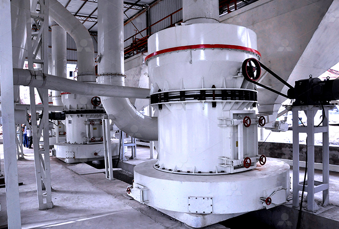
MTW European Type Trapezium Mill
Input size:30-50mm
Capacity: 3-50t/h
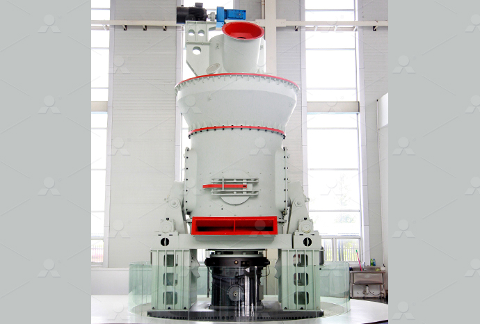
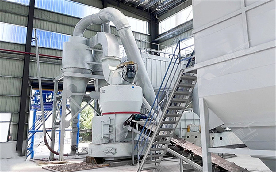
LM Vertical Roller Mill
Input size:38-65mm
Capacity: 13-70t/h
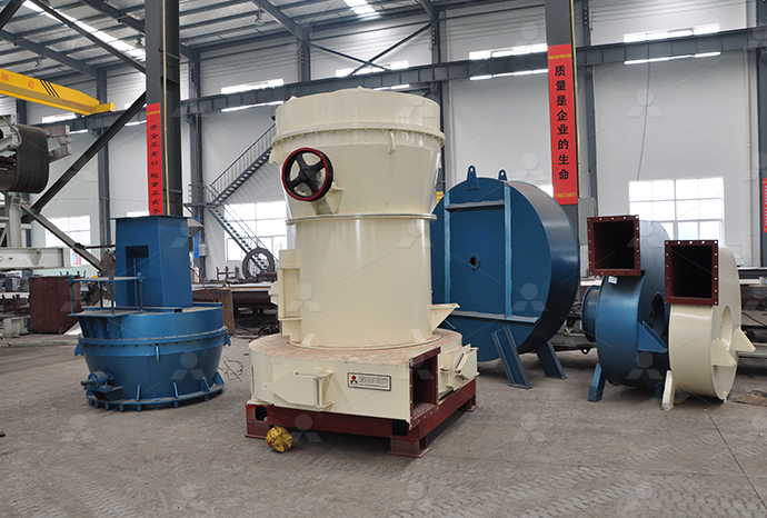
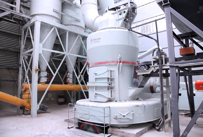
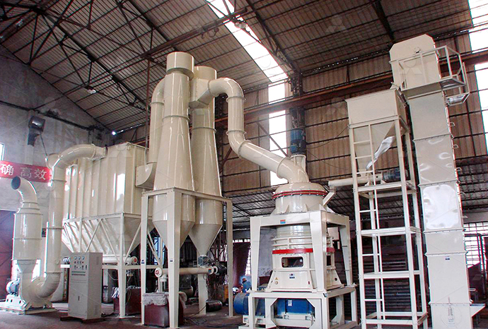
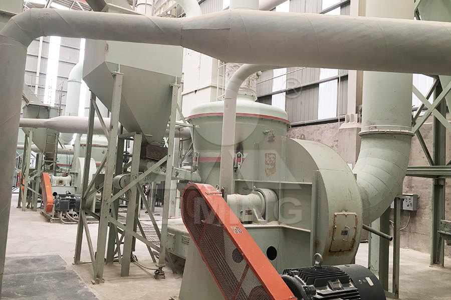
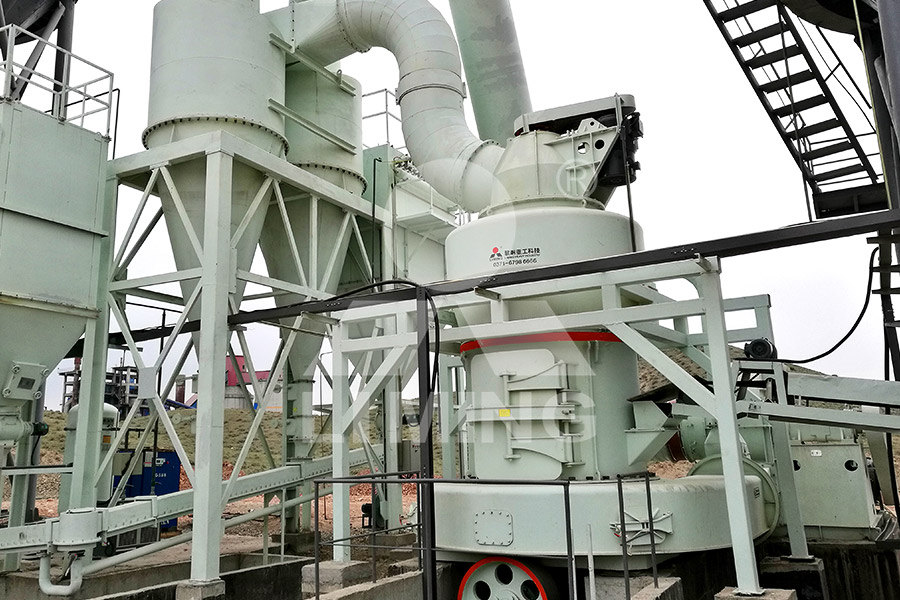
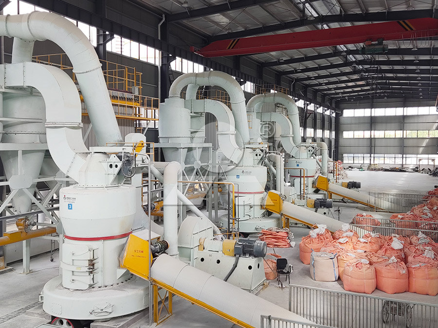
Raymond Mill
Input size:20-30mm
Capacity: 0.8-9.5t/h

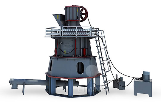
Sand powder vertical mill
Input size:30-55mm
Capacity: 30-900t/h
LUM series superfine vertical roller grinding mill
Input size:10-20mm
Capacity: 5-18t/h
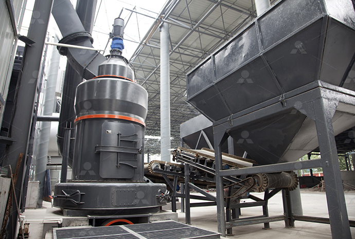
MW Micro Powder Mill
Input size:≤20mm
Capacity: 0.5-12t/h

LM Vertical Slag Mill
Input size:38-65mm
Capacity: 7-100t/h
LM Vertical Coal Mill
Input size:≤50mm
Capacity: 5-100t/h
TGM Trapezium Mill
Input size:25-40mm
Capacity: 3-36t/h
MB5X Pendulum Roller Grinding Mill
Input size:25-55mm
Capacity: 4-100t/h
Straight-Through Centrifugal Mill
Input size:30-40mm
Capacity: 15-45t/h
What is the contact surface between the pad and the pad
What is a PCB Pad: Everything You Should Know About
For example, an axial leaded resistor needs a round pad with a hole, while a surface mount chip capacitor utilizes rectangular pads The size, shape, pitch, and layout of pads must align with the leads or pads on the component 2024年11月13日 In simple terms, a PCB pad refers to the lead holes on the PCB board and the surrounding copper skin (copper foil) of different shapes What are the types of PCB pad? There are two types of pads in the board: The complete guide to PCB pad :types, size, spacing, Electrical Contact Pad is a conductive area on a PCB (Printed Circuit Board) used to connect electronic component pins or wires The pad is usually made of copper and is plated (such as tin or gold) to enhance its conductivity and corrosion Electrical Contact Pads in PCB : Varieties, Architecture, 2024年11月5日 PCB pads, essential for electronic connectivity, serve as connection points and aid heat dissipation Throughhole pads suit pin insertion, while surface mount pads are for smaller components Varied pad shapes PCB Pad Fundamentals: Concepts, Types, and Design
Working with Pads Vias Altium
2024年10月21日 The key difference between a via and a pad is that as well as being able to span all layers of the board (top to bottom), a via can also span from a surface layer to an internal layer or between two internal layersContact pads or bond pads are small, conductive surface areas of a printed circuit board (PCB) or die of an integrated circuit They are often made of gold, copper, or aluminum and measure Contact pad Wikipedia2024年6月30日 PCB pads are the metallic surfaces that connect various PCB components in the board Understanding them is crucial while manufacturing PCBs for an electrical device This blog will cover all the aspects related to What is PCB Pad? Design, Types, Functions LionCircuits2023年9月19日 Soldering is one of the most important processes in PCBA processing On printed circuit boards, electrical connections to all components are made via PCB padThe pads are a very critical part of the PCB that The complete guide to PCB pad :types, size, spacing,
What is a PCB pad – different types and design
2023年1月24日 What is a PCB pad? A Printed Circuit Board (PCB) pad is an area of copper that has been etched onto a board in order to make contact with components It is typically rectangular, oval, or round and acts as a point of The minimum width of the soldering ring of PAD is 020 mm to ensure the adhesion of the pad Viainpad When the circuit board size is limited, the design components have smaller PCB footprints, component densities increase, so What Is the Difference Between Via and Pad in PCB?2024年6月30日 Surface Mount Pad SMD pads are pads which are intended for use in surface mounting of the components These pads enable the components to be soldered on the surface of the PCB without their leads passing through the holes They offer advantages such as smaller footprint, higher component density, and easier automated assembly processesWhat is PCB Pad? Design, Types, Functions LionCircuits2022年3月9日 Pad printing, which uses a flexible silicone pad to transfer ink from an etched base plate onto the product, is ideal for moving a 2D image onto a 3D object And it’s a particularly effective method for printing onto irregular, small objects such as keyrings and jewelry where screen printing may strugglePad Printing vs Screen Printing What's the Difference? Xometry
Surfacewetting characterization using contactangle Nature
2018年7月9日 Wetting, the process of water interacting with a surface, is critical in our everyday lives and in many biological and technological systems The contact angle is the angle at the interface where 2021年2月7日 Without regeneration of the pad surface during polishing, the rate of material removal rapidly reduces over timeBy evaluating the deterioration of the pad surface during polishing, the (PDF) Analysis of Correlation between Pad Temperature and 2017年4月2日 contact with the cliché, hampering ink pickup Again, the more rolling action that is achieved, the more ink • Irregular ink pickup during the test print usually means that air is being trapped between the pad surface and the cliché Watch carefully as the pad is being imaged to be sure that a rolling action is occurringUnderstanding The Pad In Pad Printing2011年1月15日 Research highlights The actions of the ultrasonic and silica abrasive particles were the main factors in the sapphire material removal rate (MMR) The chemical additives were helpful to decrease the roughness of sapphire The effects of the flexural vibration on the interaction between the silica abrasive particles, pad and sapphire substrate improved the Effects of the ultrasonic flexural vibration on the interaction between
A Guide to Thermal Interface Materials RS Components
2022年11月22日 Paste can adapt to the surface texture, whereas pads will compress to the surface, just not providing quite as tight coverage as thermal paste Another difference is in ease of application Thermal pads are relatively straightforward to use They typically have a sticky backing that must be peeled off, then the pad can simply be placed into between the line contact of the cylindrical type and point contact of the spherical type This implies that the point contact may induce a larger friction force between the pad and pivot, thereby a ecting the dynamic states Childs and Harris [7] introduced an equivalent spring model composed of a fluid lubricant filmE ects of Tilting Pad Journal Bearing Design Parameters on the Pad 2022年1月3日 If galvanic isolation is not required, metal fillers such as silver can also be used In order to reduce the contact resistance, a certain amount of pressure between the interfaces is required This pressure then compresses Choosing the right thermal interface material: paste, 2019年9月29日 This is the extra diameter of a capture pad over the minimum pad size needed to exactly “capture” the shadow cast by the drilled hole This extra copper is used to make a connection between a trace entering a pad Pad Stack Design And The Fabrication Process—part 1
Working with Pads Vias Altium Designer 25 Technical
2024年10月21日 Vias are circular in the X and Y planes, like round pads The key difference between a via and a pad is that as well as being able to span all layers of the board (top to bottom), a via can also span from a surface layer to an 2024年5月23日 Do you know what SMD (Solder Mask Defined) and NSMD (NonSolder Mask Defined) are? What is the difference between SMD and NSMD? What are the advantages and disadvantages of SMD and NSMD? When should they be used?Many people may say that they are in the PCBA electronics industry and have heard of SMD (Surface Mount Device) The difference between SMD and NSMD pad design, advantages 2015年7月10日 Typically thermal pads are used when a pad is connected to a plane and a component lead will be soldered to the pad Thermal pads improve the solderability of the pad, reducing the chance of a “cold solder joint” A solid pad requires more heat to solder the connection because there is more surface areaWhat is the difference between a thermal pad and a solid pad?Pad Surface 3Dimensional Data Pad Surface Height Distribution Pad Bulk Pad Surface + 2 Adapted from: AS Lawing, Topics in Plasma Science and Thin Film Applications III in Honor of Herbert H Sawin AIChE Conference, Philadelphia, November 17, 2008Advances in CMP Pad Conditioning American Vacuum Society
.jpg)
Pad Printing: The Process, its Advantages, and Applications
2019年10月12日 Activating a New Printing Pad Before you use the printing pad for the first time, it is important to deoil them carefully To do this, soak some thin paper towels in ink thinner and gently wipe down the surface of the custom pad Rough or dry scrubbing of the automated pad will easily damage the printing pad surfaceExample \(\PageIndex{1}\) A disc sander is pressed against a wooden surface with a force of 50 N Assuming the kinetic coefficient between the sanding pad and the wood is 06 and the diameter of the sanding disc is 02 meters, what is the torque the motor must exert to keep the disc spinning at a constant rate?66: Disc Friction Engineering LibreTexts2022年4月14日 To obtain a performance improved dry electrode for bioelectrical activity detection is still a challenge, which is mainly due to the poor fundamental understanding on the impedance of the electrode–skin interface Herein, the impedance between the electrode and the skin interface of three types of electrodes, which are the wet electrode, semidry electrode, and Insight into the Contact Impedance between the Electrode and 2017年1月31日 The pad is clamped at its edges in the orthogonal plane on the contact surface, there by permitting a rigid body movement in the normal direction to the contact surface, such that found in automotive brake assembly Fixed support of the outer pad The mechanical loading is represented by the pads pressing on to the rotating disc, generating Predictive modeling and simulation of the structural contact
What Are PCB Pads? The Ultimate Guide to Types,
2024年6月28日 The standard pad size for a PCB varies based on the component and the type of pad For throughhole components, pad sizes typically range from 15 to 2 times the lead diameter For surface mount components, 2 Circular padswidely used in single and doublesided printed boards with regularly arranged components 3 Islandshaped padthe connection between the pad and the pad is integrated, and it is often used in vertical irregular arrangement 4 Teardrop padsoften used when the connected traces are thinner, and are often used in highfrequency What are the design standards for pad shape and size in A 2006年3月15日 Hello every one Could it be possible for some one to give a breif description of Pin and pad and wat is the difference between them and pattern on printed circuits designated for the mounting or attachment of components,it can be either through hole or Surface mount devices Facebook Twitter Contact us Online statisticsWhat's the difference between pin and pad Forum for 2022年6月5日 A hard mouse pad, like the Logitech G440 Hard Gaming Mouse Pad, is usually made out of plastic, metal, or glass to provide a smooth, level surface Due to lack of friction, they're great for gamers or anyone who wants or needs to move their mouse fast With the speed and ultrasmooth surface, it'll be harder to control your mouse with precisionHard vs Soft Mouse Pad: Which Is Better? HowTo Geek
.jpg)
What is a Pad in PCB Design? JHYPCB
2024年1月8日 – Pads serve as soldered interface between component pins and PCB traces – Various pad shapes exist to accommodate throughhole and SMT parts – Pad size, positioning and spacing impacts manufacturability – Electrically, pads propagate signals and power within the circuit – Mechanically, pads ensure components stay fixed to board surfaceIn fact, to increase the contact surface useful for the passage of the current, it is possible to choose a knurled pad instead of a classic smooth and slightly concave pad traditionally used Choosing a knurled pad has multiple advantages: • Multiple points of contact between the surface of one pad and the otherTHE CONTACT RESISTANCE OF THE ELECTROMECHANICAL RELAY2024年5月1日 This study investigates the frictional and surface strain behaviour of silicone hemispherical finger pad simulants with different stiffness during tribological interactions with a smooth glass plate A novel contact area and strain measurement method employing a digital image correlation technique was employed to give new understanding of the pad behaviour The Effect of Stiffness on Friction, Surface Strain and Contact Area 2016年5月4日 For example, as an excellent lubricant, graphite can decrease wear rate effectively by reducing the direct contact between surface of friction material and brake disk 14 However, the abrasive (eg metal sulfide) is generally used to increase friction coefficient and strengthen wear resistance of friction material •Review on the friction and wear of brake materials
Simulation of wear and contact pressure distribution at the pad
2009年12月1日 A more correct procedure would be to assume that the pad surface is worn in the inwards direction of its local surface normal, which may vary over time due to uneven wear over the contact surface The simplification is justified by the fact that the two contact surfaces are initially flat and conformal, and that the expected wear depth is much smaller than the 2020年7月16日 Once the gold layer is not enough to protect the nickel layer, causing nickel to contact with the air to corrode and oxidize or be eroded by gold water transition, it will form the socalled black pad phenomenon, and at this The Formation and Prevention of Black Pad and 2008年1月1日 Irregular ink pickup during the test print usually means that air is being trapped between the pad surface and the plate Watch carefully as the pad is being imaged to be sure that a rolling action is occurring Whenever Understanding the Pad in Pad Printing Plastics 2023年8月30日 What is the purpose of a mattress pad? The purpose of a mattress pad is to modify the firmness level at the surface of the mattress This can make the mattress softer or firmer A mattress pad can also serve as a What Is a Mattress Pad? — Do You Need One?
A Study on the Correlation between Pad Property and Material
2011年4月25日 tried to investigate a real contact area (RCA) between pad and wafer according to pad roughness, Rku by measuring asperities of the pad surface using confocal microscope Furthermore, authors tried to find a good correlation between pad property and MRR in CMP process 2 Experiment 21 Pad surface2023年11月3日 Set up the pad printing machine, ensuring it’s clean, calibrated, and in optimal working condition Adjust the ink cup and doctor blade The ink cup contains the ink, and the doctor blade ensures the cliché’s surface is properly Pad Printing: The Process, Advantages, and Applications2023年5月5日 Step 4: The pad is raised and the bottom layer of ink on the pad again comes into contact with air and becomes tacky To stick on the substrate when the pad is pressed against it Step 5: The pad moves forward towards the object and the spatula moves with it to spread a new layer of ink on the printing platePad Printing Finish: Process, Types, Benefits and UsesPad printing is a very dynamic printing method that can be applied to a large number of products: Pad printing is typically used for applications that require print quality, precision or a complex shape Medical devices (syringes, surgical instruments, etc) Implantable and bodyworn medical devices (catheter tubes, contact lenses, etc)What is pad printing? The Print Blog
.jpg)
IVD Lateral Flow – Sample, Conjugate and Absorbent Pad Basics
S ample, C onjugate, and A bsorbent Pad M aterials Lateral flow pad materials comprise the porous matrices that are used for the sample pad, conjugate pad, and absorbent pad Most commonly, cellulosic materials (ie, filter papers) are used for sample and absorbent pads, while glass fiber filters are used for the conjugate padWe offer a range of cellulosic and glass fiber Download scientific diagram Contact area ratio between a rough pad and a smooth, flat surface versus plasticity index, for p = 35 kPa and H a = 290 MPa from publication: The Role of Pad Contact area ratio between a rough pad and a smooth, flat surface 2022年1月1日 However, for pads, the major design and response issues reduce to (a) control of global compliance, particularly at the wafer edge, (b) improvement in pad contributions to planarization efficiency and feature recess, (c) regulation and reduction of pad modulus to reduce contact stress for defect reduction, and (d) design of efficient liquid and polishing byproduct CMP pads and their performance ScienceDirect